Deploying specialized heavy-copper core boards and high-conductivity architectures designed to sustain peak currents and massive heat dissipation requirements within heavy industrial installations across Metro Manila.
Metro Manila, alongside adjacent high-tech hubs like the CALABARZON economic zones, is rapidly transitioning into a regional powerhouse for telecommunications, renewable energy grids, and data centers. As local telecommunications companies deploy widespread 5G networks, and multi-tenant data center campuses break ground across the city, the demand for power delivery systems has reached unprecedented thresholds. This transition requires extreme thermal management and massive current load handling capabilities, which standard PCBs simply cannot support.
This is where Thick Copper PCBs (Heavy Copper PCBs) enter the picture. By utilizing copper weights ranging from 3oz/ft² to upwards of 10oz/ft², these specialized circuit boards act as both power distribution networks and structural foundations for heavy-duty switching systems. Their application extends from local solar inverter installations to high-capacity DC fast-charging grids built for electric vehicles running along Manila’s arterial expressways.
Operating high-frequency, high-amperage systems in tropical climates like the Philippines presents distinct challenges. High ambient temperatures combined with high humidity lead to rapid heat accumulation in electrical enclosures. Standard FR4 boards with thin copper tracks (1oz or 2oz) experience severe copper migration, delamination, and solder joint fractures under continuous thermal cycling.
By deploying heavy copper traces, designers can establish a direct, low-resistance path for high-power electronics. The massive cross-sectional area of the copper traces facilitates horizontal thermal spread, preventing localized "hot spots" that degrade semiconductor components. Furthermore, the robust mechanical composition of thick copper substrates ensures structural durability when mounted inside demanding environments like mining machinery or industrial manufacturing units in regional economic zones.
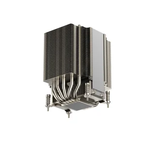
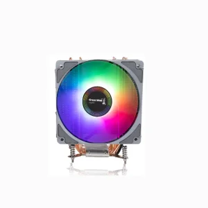
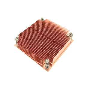
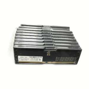
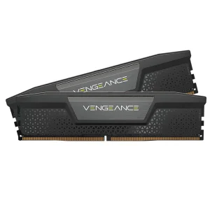
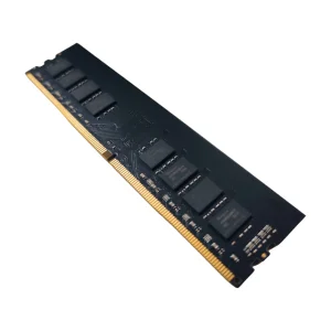
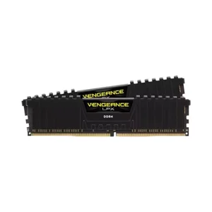
High-performance passive heat dissipation assemblies, specialized coolers, and legacy memory architectures to support high-duty industrial servers and localized processing nodes.
Fabricating PCBs with thick copper traces requires specialized chemical processes that differ vastly from standard printing. A primary challenge in thick copper manufacturing is differential etching. When acid etches down through thick copper layers, it naturally wants to undercut the sides of the traces. This requires advanced lithography parameters and compensated trace designs to ensure that the trace maintains the correct width at the base and does not compromise current carrying capacity.
Additionally, applying the solder mask to a board with 3oz to 10oz traces requires multiple screen-printing steps. Standard single-pass liquid photoimageable (LPI) solder masks cannot adequately coat the steep walls of thick copper traces, leaving them vulnerable to short circuits. A multi-layer LPI deposition process is utilized, followed by specialized curing profiles, to build up a protective barrier over the corners of all high-power traces.
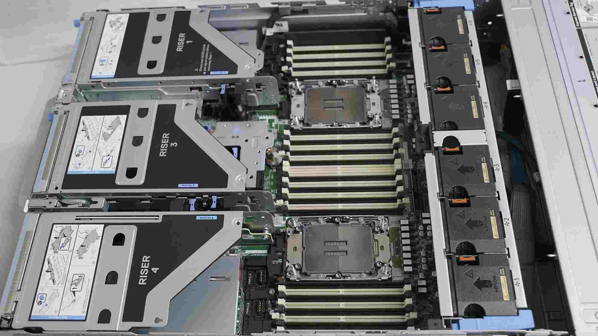
As telemetry systems, processing controllers, and server motherboards demand more compact structures, integrating heavy copper power planes with fine-pitch signal layers (HDI) is a key area of development. This hybrid approach uses standard, thin-copper signal layers in internal stacks for high-speed processors, while burying thick copper traces in the core layer for power distribution. This saves structural space and eliminates the need for external busbars.
VoltDRAM Semiconductor Co., Ltd. coordinates its production through our advanced Chinese manufacturing base. This facility spans 320–480㎡, incorporating computerized testing facilities and highly automated SMT assembly lines. With an annual export revenue of USD 8–18 million, our plant is built to support both large-scale production runs and high-mix, low-volume custom orders.
Our production facility utilizes rigorous Quality Management Systems. Every batch of heavy copper boards undergoes a multi-point inspection process:


A reliable electronics development partner, combining extensive export capability, technical expertise, and solid supply chain networks to provide resilient manufacturing solutions.
For organizations operating within the Philippine Economic Zone Authority (PEZA) tax-free enclaves in Laguna, Cavite, and Clark, logistics efficiency and regulatory compliance are essential for smooth production. We provide comprehensive import documentation, including certificate of origin declarations, material compliance reports (RoHS & REACH), and custom tariff classification codes (HS Codes) to simplify customs processing at the Manila ports.
VoltDRAM supports clients during the development phase. Our engineering team, consisting of 60 to 300 experienced technical specialists, works directly with clients to review Gerber files, audit copper thickness against target current profiles, recommend optimal surface finishes (ENIG, Immersion Silver, OSP), and coordinate prototype development quickly.
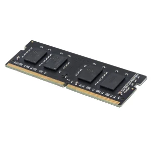
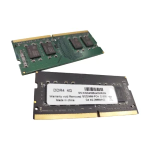
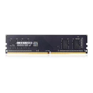
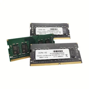
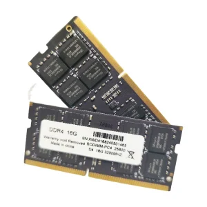
Standard and high-performance memory modules optimized to support high-density industrial control units and enterprise computing systems in Metro Manila.
Technical details and answers regarding thick copper electronics design, standards compliance, and logistics pipelines from VoltDRAM.
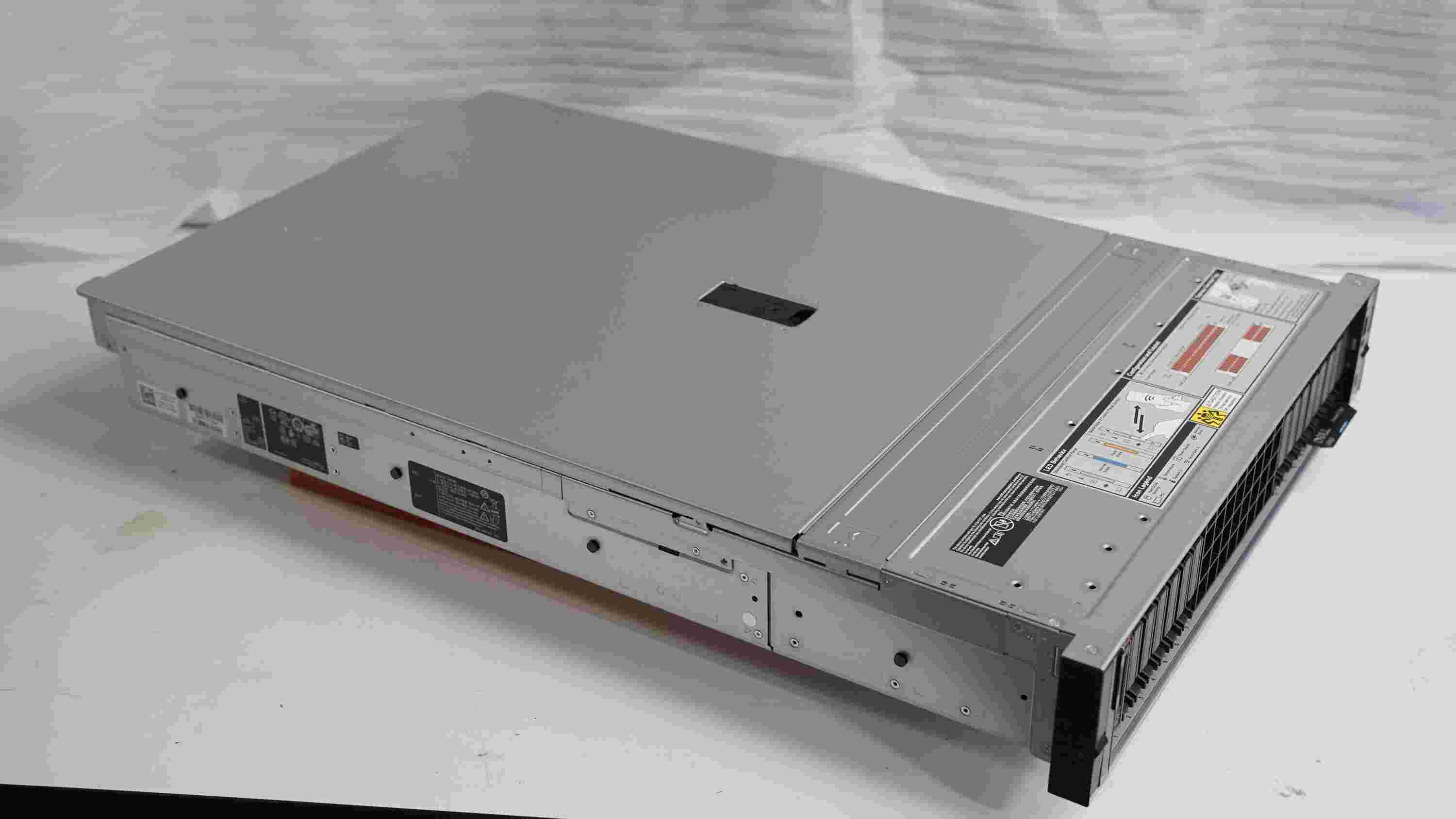
A Thick Copper PCB (commonly referred to as a heavy copper PCB) features copper conductors with weights ranging from 3oz/ft² to over 10oz/ft². Standard PCBs typically use 1oz or 2oz copper weights. Thick copper boards are needed when circuits must carry large electrical loads (exceeding 20-30 Amps continuously) or when components generate significant heat, such as in high-voltage industrial solar converters, electric vehicle (EV) charging units, power distribution networks, and industrial server power supplies.
Copper has a Coefficient of Thermal Expansion (CTE) of approximately 17 ppm/°C, while standard FR4 resin substrate expands much faster in the vertical (Z-axis) direction (around 50-80 ppm/°C). When exposed to continuous thermal load, this CTE difference can strain internal connections and solder joints. To address this risk, we use high-Tg (glass transition temperature) laminates, such as Tg 170°C or Tg 180°C, and implement thermal vias to distribute heat horizontally. This maintains physical stability and performance in warm, humid conditions like those in Manila.
For shipments to Philippine Economic Zone Authority (PEZA) enclaves like those in Laguna Technopark or Cavite Economic Zone, we offer optimized import processing. Production typically takes 7 to 15 working days depending on trace complexity. Sea freight from our southern China facility to the Manila Port takes 5 to 7 days, while urgent air freight orders are delivered in 2 to 4 days. We provide comprehensive import documentation, including custom HS tariff codes and RoHS/REACH compliance files, to support efficient customs clearance.
Electroless Nickel Immersion Gold (ENIG) is preferred for thick copper boards because it provides a flat, coplanar surface that improves solder joint reliability for fine-pitch surface-mount (SMT) components. Hot Air Solder Leveling (HASL) can result in uneven surfaces on thick copper traces due to the surface tension of molten solder over steep trace edges. Additionally, ENIG's nickel barrier layer prevents copper migration at high operating temperatures, ensuring long-term connection integrity.
Yes, we design and manufacture hybrid multi-layer PCBs that combine different copper weights. The internal core layers can feature 3oz or 4oz copper planes for high-power distribution, while the outer layers use standard 1oz copper for fine-pitch, high-speed signals (such as DDR routing or RF signals). This hybrid design improves power transmission while maintaining clean signal routing on a single board, reducing physical space requirements.
All products, including PCBs, motherboards, heat sinks, and DDR memory modules, undergo strict quality control. Memory modules go through automated optical inspection (AOI), electrical speed checks, and long-term burn-in testing to ensure stability. PCBs undergo flying probe electrical tests, micro-section analysis to verify copper plating thickness in the vias, and thermal stress tests to confirm material stability before shipment.