In the rapidly evolving landscape of telecommunications, aerospace, and high-performance computing, the transmission of digital signals is no longer bounded by traditional circuit dynamics. As operational frequencies breach the gigahertz (GHz) thresholds—driven by 5G NR (New Radio), millimeter-wave (mmWave) applications, automotive ADAS (Advanced Driver Assistance Systems) radar systems, and aerospace transceivers—the physical printed circuit board (PCB) transitions from a passive mechanical substrate to an active electrodynamic component.
High-Frequency PCBs are engineered to mitigate signal attenuation, minimize electromagnetic interference (EMI), and maintain phase consistency across ultra-wide bandwidths. The design and manufacturing processes of these specialized boards dictate the reliability and efficiency of critical wireless communication channels. As global industries demand higher throughput and lower latencies, the reliance on high-frequency, high-speed substrates has transitioned from a niche design option to a global technological mandate.
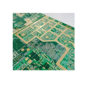
To address these complexities, developers leverage high-performance laminates such as PTFE-based Rogers materials, Taconic TLY-5, and Shengyi high-TG FR4. The mechanical stack-up configuration—often incorporating mixed-dielectric lamination (also known as hybrid pressure stacks)—combines cost-effective FR4 with highly expensive RF laminates, maximizing structural rigidity and signal propagation velocities while maintaining budget viability.
Procuring high-frequency PCBs presents unique challenges that extend beyond typical lead times and unit costs. Enterprise buyers, server system architects, and defense procurement agents are forced to evaluate the complete trace lifecycle, material availability, and factory verification metrics to ensure system reliability.
The primary metric of concern is the Dielectric Constant (Dk, or relative permittivity, εr). Fluctuations in Dk alter the characteristic impedance of transmission traces, inducing signal reflection, phase shifts, and data corruption. High-end applications require Dk values to be controlled within a tolerance of ±0.05. The loss tangent (Df), representing the electrical energy dissipated as heat in the substrate, must remain exceptionally low (typically between 0.0009 and 0.003) to preserve signal strength across extended path runs.
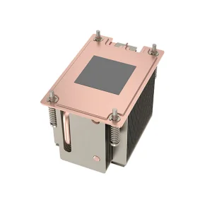
Because RF power amplifiers, memory registers, and computing modules generate massive heat signatures, materials must possess closely matched Coefficients of Thermal Expansion (CTE). If the CTE of the copper cladding deviates significantly from that of the underlying dielectric material, the resulting shear stresses during thermal cycling can lead to delamination, micro-cracks in blind/buried microvias, and intermittent connection failures. In hybrid stackups, matching the Z-axis CTE of FR-4 and Rogers/Taconic sheets is critical to passing rigorous thermal shock testing.
As the global semiconductor and electronics hardware market demands faster time-to-market cycles, the integration of advanced manufacturing paradigms becomes vital. China’s Factory 4.0 infrastructure provides a template for high-precision, low-waste PCB fabrication and PCBA assembly.
VoltDRAM Semiconductor Co., Ltd. represents this state-of-the-art manufacturing synergy. Operating a specialized 320–480㎡ manufacturing facility containing automated processing environments, VoltDRAM has spent 8–15 years in the semiconductor memory development industry and has accumulated 6–9 years of pure export experience. Producing between USD 8–18 million in annual export revenue, VoltDRAM caters to strict global standards, shipping to North America, Europe, Southeast Asia, and the Middle East.
VoltDRAM designs and launches 120–450 new product variants yearly, supported by an internal R&D engineering pool of 60–300 engineers. This rapid cycle matches the speed requirements of evolving RF system boards.
Quality is backed by 35–80 experienced inspectors employing Automated Optical Inspection (AOI), high-frequency electrical performance simulation, burn-in testing, and reliability stress screening under strict ISO conditions.
VoltDRAM maintains structural links with over 600–1,500 supply chain partners, guaranteeing uninterrupted access to raw materials, including Rogers substrates and high-grade copper foils.
To achieve maximum operational efficiency, designers must select materials suited for their target band. Selecting Rogers for millimeter-wave backhaul or Shengyi High TG170 for multi-layered computing applications dramatically changes signal performance metrics.
| Material Class / Name | Dielectric Constant (Dk @ 10 GHz) | Loss Tangent (Df @ 10 GHz) | Glass Transition Temp (Tg) | Primary Commercial Use Cases |
|---|---|---|---|---|
| Rogers RO4000 Series | 3.38 – 3.55 (± 0.05) | 0.0021 – 0.0027 | > 280 °C | Cellular Base Station Antennas, ADAS Automotive Radar, LNBs |
| Taconic TLY-5 (PTFE Based) | 2.20 (± 0.02) | 0.0009 | 280 °C (N/A) | Aerospace Telemetry, Satellite Communications, Phase Shifters |
| Shengyi FR-4 High TG170 | 4.60 (± 0.15) | 0.0150 | 170 °C | High-Speed Digital Logic, Motherboards, Power Supplies |
| Hybrid Lamination (FR-4 + Rogers) | Variable (Mixed Layering) | Localized < 0.003 | Dk/Df Dependent | Multi-channel RF Transceivers, Industrial Controls, IoT Gateways |
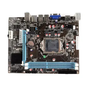
High-frequency PCBs do not operate in isolation; they serve as the neurological network for complex electronic installations. Modern system developers integrate high-frequency signals with memory and processing units to build high-efficiency edge controllers, server motherboards, and complex communication networks.
Automotive ADAS uses radar networks running on the 24GHz and 77GHz bands to execute instant collision avoidance, adaptive cruise control, and blind-spot detection. These sensor modules demand sub-millimeter microvias and uniform dielectric thicknesses. By combining a Taconic TLY-5 or Rogers laminate outer layer (where the microstrip antennas are etched) with a multi-layer FR4 internal structural support, factories can construct safe, highly durable automotive-grade sensor assemblies.
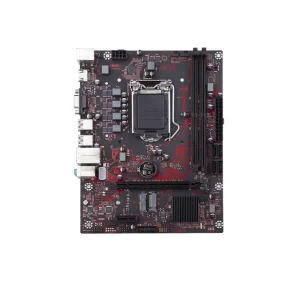
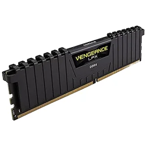
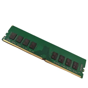
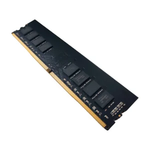
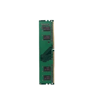
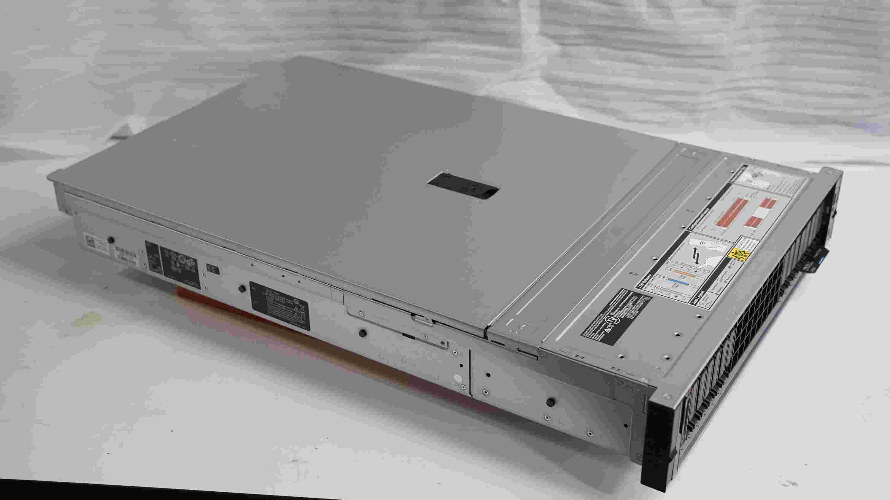
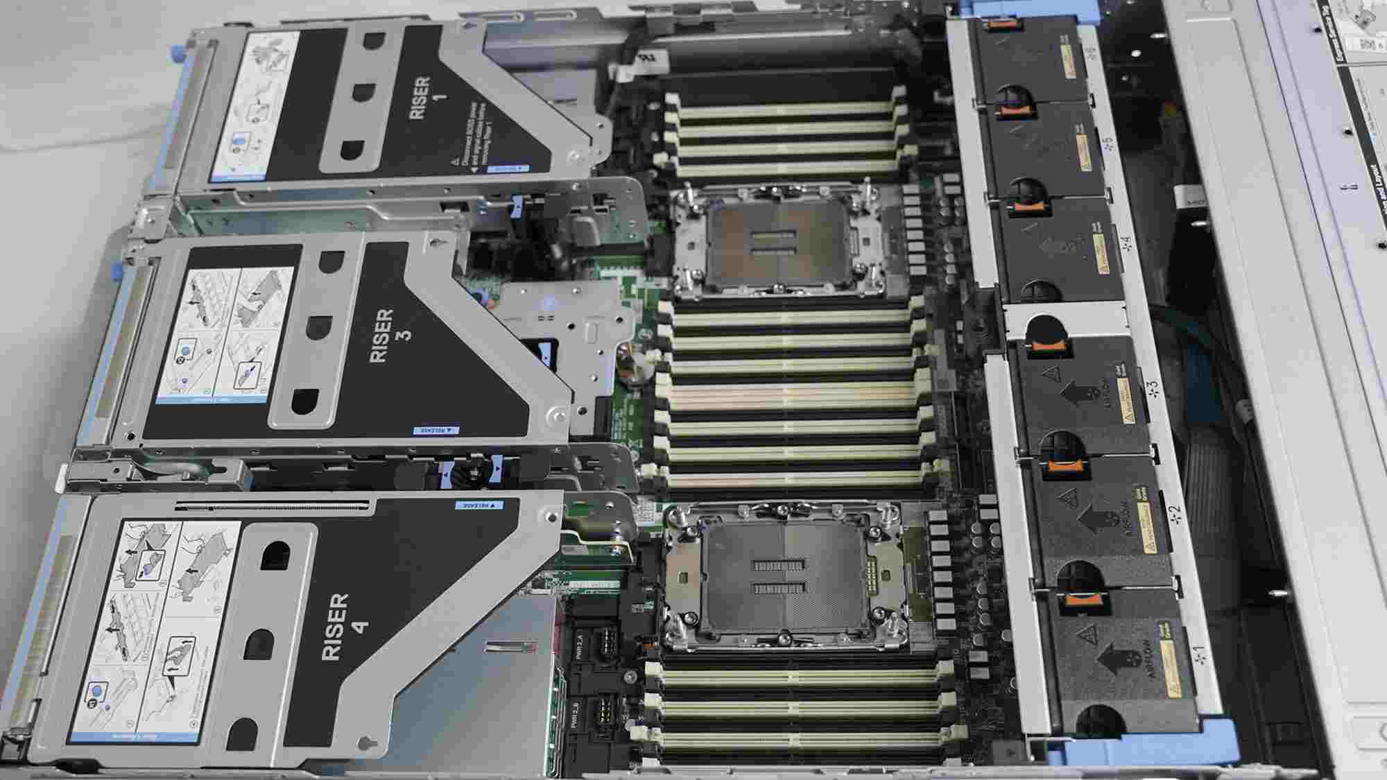
In high-density data centers, data transfer speeds are limited by the physical copper tracks running between the CPU and the system memory. Modern server motherboard configurations require high-speed channels capable of handling DDR5 performance, where data rates reach up to 6400 MT/s and above. VoltDRAM Semiconductor's specialization in DDR5 memory modules aligns with these requirements. High TG170 FR-4 mixed-pressure boards provide the structural matrix, allowing server processors and high-frequency memory modules to maintain clear signal integrity under high thermal loads.
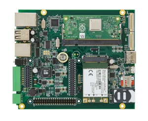
Industrial automated lines rely on compact, hardened controllers, such as custom Raspberry Pi industrial control boards, to execute real-time automation logic. These boards aggregate inputs from multiple local sensors, requiring efficient RF layout shielding to function in environments with high electrical noise. VoltDRAM's custom PCB design capability, SMT patch processing, and complete electronic assembly line (PCBA) enable industrial clients to deploy reliable hardware that resists electrical noise.
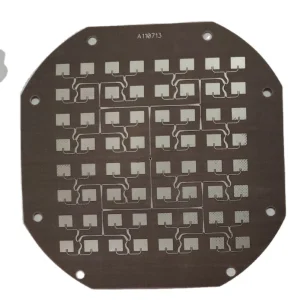
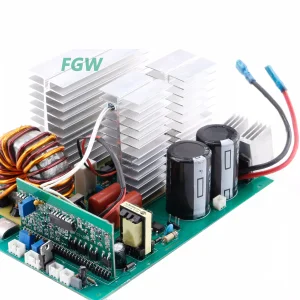
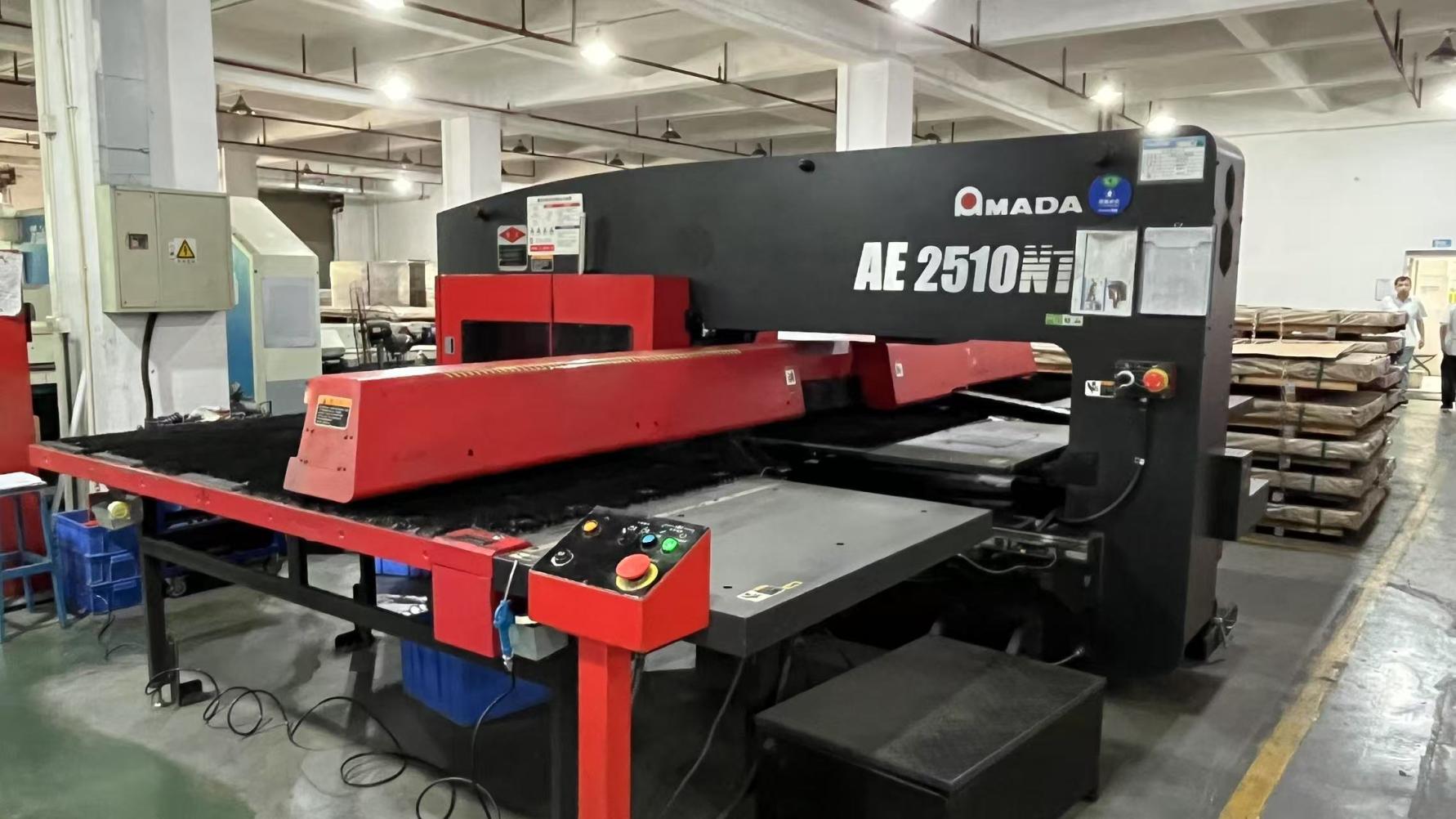
Visual documentation of our cleanroom operations, SMT assembly lines, and high-frequency validation equipment.


Hybrid stack-ups (mixed pressure) place high-performance, low-loss materials (like Rogers 4000) solely on the layers where high-speed RF routing is required, while utilizing standard FR-4 for the remaining mechanical and DC power layers. This configuration provides a balanced solution that reduces overall material costs while meeting necessary thermal, mechanical, and electrical performance benchmarks.
Water possesses a high Dielectric Constant (Dk ≈ 80). If a PCB substrate absorbs ambient moisture, its localized Dk will rise, causing impedance changes and increasing the dissipation factor (Df). Materials such as Taconic TLY-5 feature a low moisture absorption rating (<0.02%), making them suitable for marine, outdoor base station, and high-humidity environments.
Validation requires a multi-step quality control workflow: 1) Time Domain Reflectometry (TDR) to test characteristic trace impedance tolerances; 2) S-parameter analysis via Vector Network Analyzers (VNA) to measure return and insertion losses; 3) Microsectioning to verify microvia plating integrity; 4) Automated Optical Inspection (AOI) to identify circuit trace anomalies; and 5) Thermal stress testing to confirm delamination resistance.
At high frequencies, the skin effect restricts current flow to the outer skin of the copper conductor. If the copper surface is rough at the interface with the dielectric, the effective electrical path length increases, which raises conductor losses. Implementing profile-controlled copper foils, such as VLP (Very Low Profile) or HVLP (Hyper Very Low Profile) foils, is necessary to minimize attenuation in applications operating above 10 GHz.
VoltDRAM provides engineering support starting at the initial stack-up design phase. Our engineering team assists with substrate selection, impedance simulation, and thermal analysis. Once finalized, our automated SMT lines and assembly systems process prototype batches, which then undergo electrical, burn-in, and mechanical stress tests to ensure reliable production.