Original Factory High Sensitivity Electronic Circuit Board Pcb Assembly For Gold Metal Detector

Product Description

About Us

A leading manufacturer specializing in high-density multilayer printed circuit boards and specialty boards. With certifications including UL, ISO9001:2015, ISO14001:2015, CQC, IATF16949:2016, and "National Military Standard," top-quality products and services are provided. The extensive product range includes multilayer boards, impedance boards, high-frequency boards, high TG thick copper foil boards, 5G high-speed boards, buried blind via boards, aluminum-based boards, hybrid dielectric boards, HDI, rigid-flex boards, specialty boards, and customized solutions. Driven by technological innovation, the products are widely used in industries such as communication equipment, industrial control, automotive electronics, energy and power, medical devices, IoT, research institutions, aerospace, and defense. With over 19 years of experience, over 1,000 technology innovation-oriented enterprises have been served with rapid prototyping and mass production services. We are committed to delivering cutting-edge solutions and exceeding customer expectations in the dynamic electronics industry.

Main Products

PCB Product 1
PCB Product 2
PCB Product 3
PCB Product 4
PCB Product 5
PCB Product 6
PCB Product 7
PCB Product 8
PCB Product 9

Production Line and Equipment

Equipment 1
Equipment 2
Equipment 3
Equipment 4
Equipment 5
Equipment 6
Equipment 7
Equipment 8
Equipment 9

Rigid PCB Manufacturing Capability

Category Volume Production Sample Processing
Layer count - 1-68L (64 Layer)
Max thickness 10mm (394mil) 14mm (551mil)
Min line width/space (Inner layer) 2.2mil / 2.2mil 2.0mil / 2.0mil
Min line width/space (Outer layer) 2.5mil / 2.5mil 2.2mil / 2.2mil
Alignment capability (core board) ±25um ±20um
Inner layer alignment ±5mil ±4mil
Max copper 6Oz 30 oz
Hole size (mechanical drilling) ≥0.15mm (6mil) ≥0.1mm (4mil)
Hole size (laser drilling) 0.1mm (4mil) 0.050mm (2mil)
Max size (Unit size) 850mm X 570mm 1000mm X 600mm
Max size (Panel size) 1250mm X 570mm 1320mm X 600mm
Aspect ratio (Unit size) 20:1 28:1
Aspect ratio (Panel size) 25:1 35:1
Lead-free / Halogen-free Materials EM827, 370HR, S1000-2, IT180A, EM825, IT158, S1000 / S1155, R1566W, EM285, TU862HF
High-speed PCB Material Megtron6, Megtron4, Megtron7, TU872SLK, FR408HR, N4000-13 Series, MW4000, MW2000, TU933
High-frequency PCB Material Ro3003, Ro3006, Ro4350B, Ro4360G2, Ro4835, CLTE, Genclad, RF35, FastRise27
Other Materials Polyimide, Tk, LCP, BT, C-ply, Fradflex, Omega, ZBC2000
Surface Finished HAL, HAL-LF, ENIG, Immersion Tin, OSP, Immersion Silver, Gold Finger, Hard Gold/Soft Gold Plating
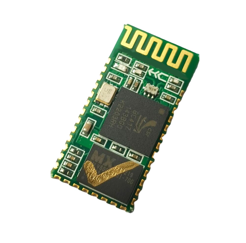
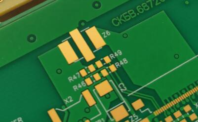
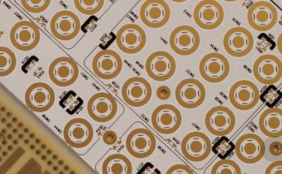
Special technology Blind & buried holes, Via in pad, Semi-plating holes, Counterbore, Step mounting holes, drill Mixed RF PCB, Busbar PCB
QUALITY ASSURANCE:
  • Consciousness of making each product a high-quality product by strictly following the quality management system.
  • Based on ISO 9001, ISO 14001, IATF16949, RoHS, REACH, UL, CQC & etc. quality management systems. Simultaneously running IATF 16949.
  • Method of involving all staff in the entire process control.
  • Objective and confidence of ensuring 100% quality.
  • Shipping acceptance criteria: Customer requirements, IPC standards.
  • Assisting customers in developing quality standards cooperating with customer experiments to improve product performance.

Laboratory Capabilities

Lab 1
Lab 2
Lab 3
Lab 4
Lab 5

Packing & Shipping

Shipping Standard
Shipping Standards:

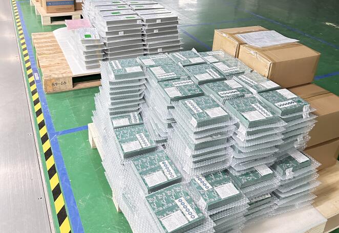
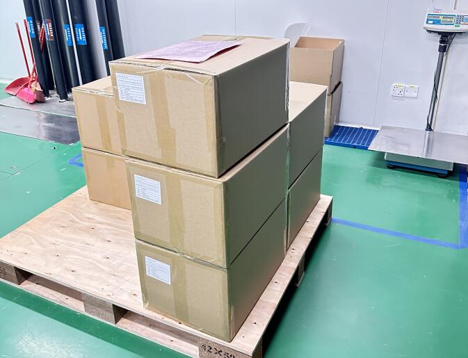
PCB orders are shipped via the following options:

  • Air ship (UPS, DHL, TNT, CTS and FEDEX)
  • Railway ship
  • Seaborne
  • Customer Designated Shipping Method
Layer Sample Shortest Lead Time Sample Standard Lead Time Mass Production Lead Time
2 layer 24 h 3 days 6-7 days
4 layer 36 h 5 days 8-10 days
6 layer 48 h 5 days 8-12 days
8 layer 72 h 5 days 9-12 days
10 layer 4 days 7 days 14 days
12 layer 4 days 7 days 16 days
14 layer 5 days 8 days 16 days
16 layer 5 days 9 days 18 days
18 layer 7 days 10 days 18 days
20 layer and above To be negotiated To be negotiated To be negotiated
Package Details 1
Package Details 2

High Efficiency Team

Professional Engineering Team
  • 24h technical support
  • 24h Gerber files handling with complete EQ within 4-8 hours
  • Support 400 new project engineering reviews
Accepted CAD/CAM Gerber Formats
  • RS-274-X & RS-274-D
  • CAD & DXP
  • Protel 99 SE
  • PADS
  • GC-CAM
Professional Manufacturing Team
  • All processes running 24 hours
  • Monthly production of more than 10K high-mix part numbers
  • More than 100 QTA orders every day
  • One-step service from prototype to mass production
Efficient Order Operation Center
  • 24 hours quick response
  • 4 hours quick response for quotation

Certifications

Quality Management Certifications

Frequently Asked Questions

Q1: What kinds of PCBs and technical services are provided?
A1: We provide a comprehensive range of PCBs including multilayer boards, impedance boards, high-frequency boards, high TG thick copper foil boards, 5G high-speed boards, buried blind via boards, aluminum-based boards, hybrid dielectric boards, HDI, rigid-flex boards, and customized solutions. We also provide engineering reviews, Gerber file handling, and rapid prototyping services.
Q2: Which certifications govern the quality management system?
A2: The quality management system complies strictly with ISO 9001:2015, ISO14001:2015, IATF16949:2016, UL, CQC, RoHS, REACH, and the "National Military Standard."
Q3: What are the primary shipping methods available for delivery?
A3: Orders can be shipped via Air (using UPS, DHL, TNT, CTS, and FEDEX), Railway, Seaborne, or any Customer Designated Shipping Method.
Q4: What is the typical lead time for PCB sample production?
A4: Sample shortest lead time is 24 hours for 2-layer boards, 36 hours for 4-layer boards, and 48 hours for 6-layer boards. The standard sample processing lead time generally ranges from 3 to 10 days depending on the layer count.
Q5: What CAD/CAM Gerber file formats are supported for manufacturing?
A5: The engineering team accepts and processes Gerber and CAD file formats including RS-274-X, RS-274-D, CAD, DXP, Protel 99 SE, PADS, and GC-CAM.
Q6: What are the limitations on layers and thickness for PCB fabrication?
A6: For sample processing, we can support up to 68 layers (64 layers for volume production). The maximum thickness supported is up to 10mm for volume production and 14mm for sample processing.

Related Products