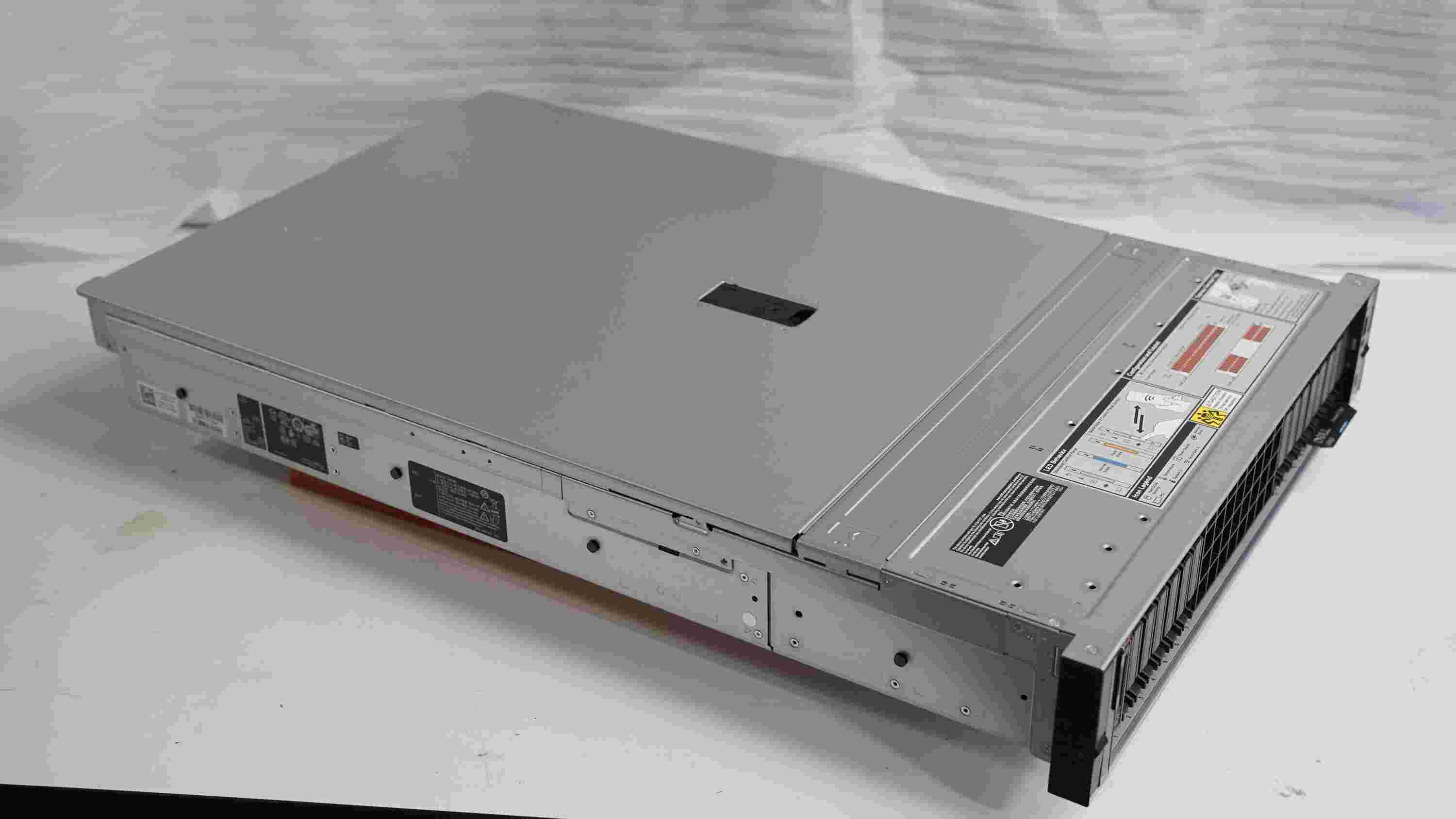
Premium heat management, double-sided breadboards, and robust computing system modules customized for Canadian thermal extremes and extreme environments.
A Technical Guide on High-Current Management, Dielectric Heat Dissipation, and Localized Industrial Applications in North American Markets.
In the PCB manufacturing landscape, "Thick Copper" (or "Heavy Copper") refers to printed circuit boards with outer and inner layer copper weights exceeding 3 ounces per square foot (oz/ft²), ranging all the way up to 20 oz/ft² or more. Standard consumer boards typically leverage 1 oz/ft² or 0.5 oz/ft² foil layers. The transition to heavier copper is not merely a scaling of dimensions; it is a fundamental shift in electrical engineering, thermal design, and manufacturing tolerances.
By using thick copper cores and traces, circuits can handle massive currents (hundreds of amperes) without overheating. This high-capacity power routing eliminates complex wiring bundles and busbars, allowing engineers to incorporate control circuits and heavy power circuits onto a single, compact, integrated multilayer board.
"The integration of heavy copper into standard multi-layer FR4 or polyimide matrices changes the thermal resistance formula of the entire system. Instead of fighting heat accumulation through massive external enclosures, thick copper structures act as integrated heat-spreaders directly underneath high-power semiconductor packages."
— Thermal Engineering Journal, Canadian Green Power Grid Initiative
The calculation of current capacity in thick copper traces must account for temperature rise constraints. Unlike thin foil circuits where empirical formulas like IPC-2152 are relatively simple, heavy copper boards require precise modeling of thermal pathways through the dielectric and to the surrounding air. Factors such as cross-sectional area, current density, ambient thermal boundaries, and plating uniformity determine the reliability of the copper run over the system's operational lifespan.
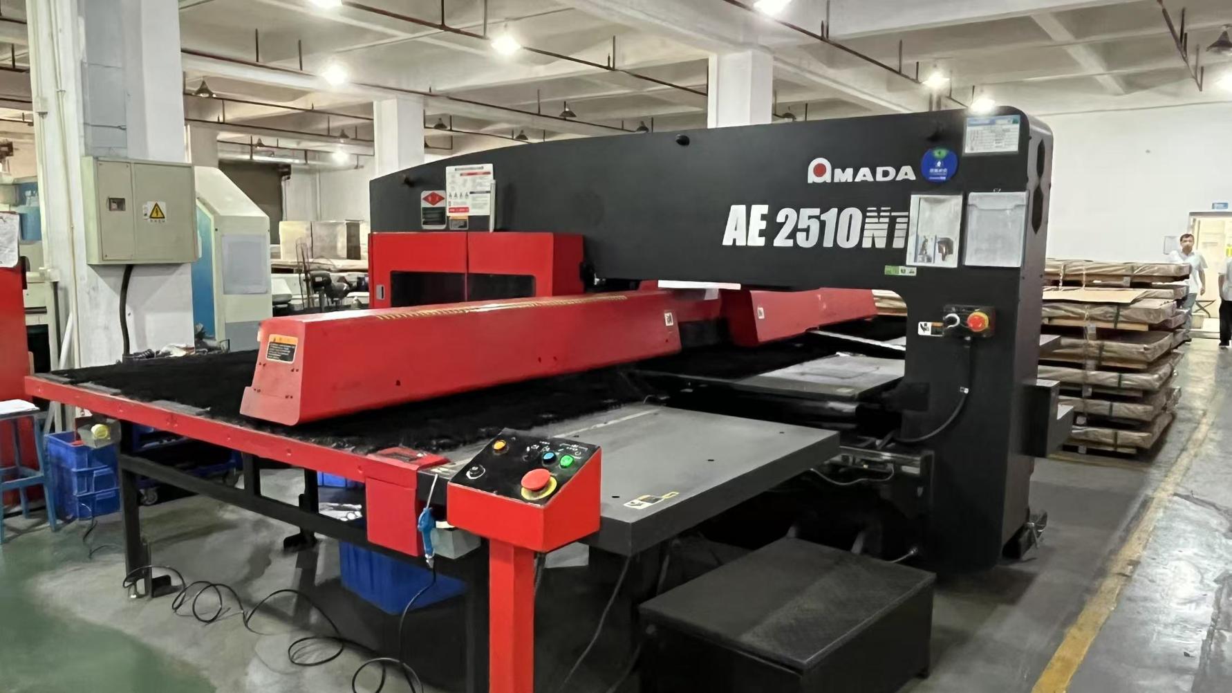
Achieving uniform electroplating thickness across a large 6 oz/ft² structure is a major challenge for factories. Without proprietary current shielding, specialized organic additives, and automated reverse pulse plating processes, outer traces can suffer from excessive edge buildup (referred to as the "dog-bone effect"), while inner features remain under-plated. This affects electrical resistance and impedance parameters, highlighting the value of partnering with premium manufacturing facilities.
Copper Thickness Range
High-Temperature Reliability
Trace Impedance Deviation
Military & Industrial Standards
Canada’s modern industrial base relies on robust electronic systems that can operate in harsh climates and under demanding physical conditions. From the sub-zero resource extraction fields of Alberta and Nunavut to the automotive design centers in Southern Ontario, thick copper PCBs provide the foundation for several localized applications:
Canada is a global leader in clean energy, generating vast amounts of hydroelectricity and wind power. Large-scale power inverters, converters, and grid control nodes require heavy copper PCBs (ranging from 4 oz to 12 oz) to manage high voltage and current inputs, ensuring stable operation in regional networks.
In the oil sands of Alberta and northern mining operations, electronic controls are exposed to constant mechanical vibration and extreme temperature swings. Heavy copper boards improve mechanical strength at solder points, preventing joint fatigue while supporting high-power mining tools and heavy machinery.
With massive investment in Canada’s EV battery belt (spanning Ontario and Quebec), local Tier-1 suppliers require reliable heavy copper PCB partners. These boards are critical for Battery Management Systems (BMS), localized high-voltage charging stations, and traction controllers.
For Canadian firms, securing these heavy-duty circuit boards presents unique sourcing challenges. Local Canadian PCB factories offer quick turnaround times and facilitate IP security under ITAR or CGP guidelines. However, scaling production often requires partnering with large-scale factories overseas to balance cost, quality, and material availability.
A side-by-side technical comparison between standard FR4 circuit layouts and heavy-duty, thick copper multilayer PCBs.
| Feature / Parameter | Standard PCB Design | Heavy Copper PCB Design | Technical Impact & Benefit |
|---|---|---|---|
| Typical Copper Foil Weight | 0.5 oz - 2 oz (17.5µm - 70µm) | 3 oz - 20 oz+ (105µm - 700µm) | Enables high current carrying capacity within a compact trace footprint. |
| Max Current Carrying Capacity | < 15 Amperes | 100 - 500+ Amperes | Eliminates the need for external wire harnesses, terminal blocks, or copper busbars. |
| Thermal Resistance (Rth) | High (~ 50-70 K/W) | Very Low (< 10 K/W) | Acts as an integrated heat sink, reducing hotspot temperatures by up to 45°C. |
| Glass Transition Temp (Tg) | 130°C - 150°C (Standard FR4) | 170°C - 180°C (High-Tg / Polyimide) | Prevents board delamination during thermal cycling and high ambient temperatures. |
| Manufacturing Process | Standard Print and Etch | Specialized Plating & Differential Etch | Ensures high-integrity sidewall geometry and void-free dielectric filling. |
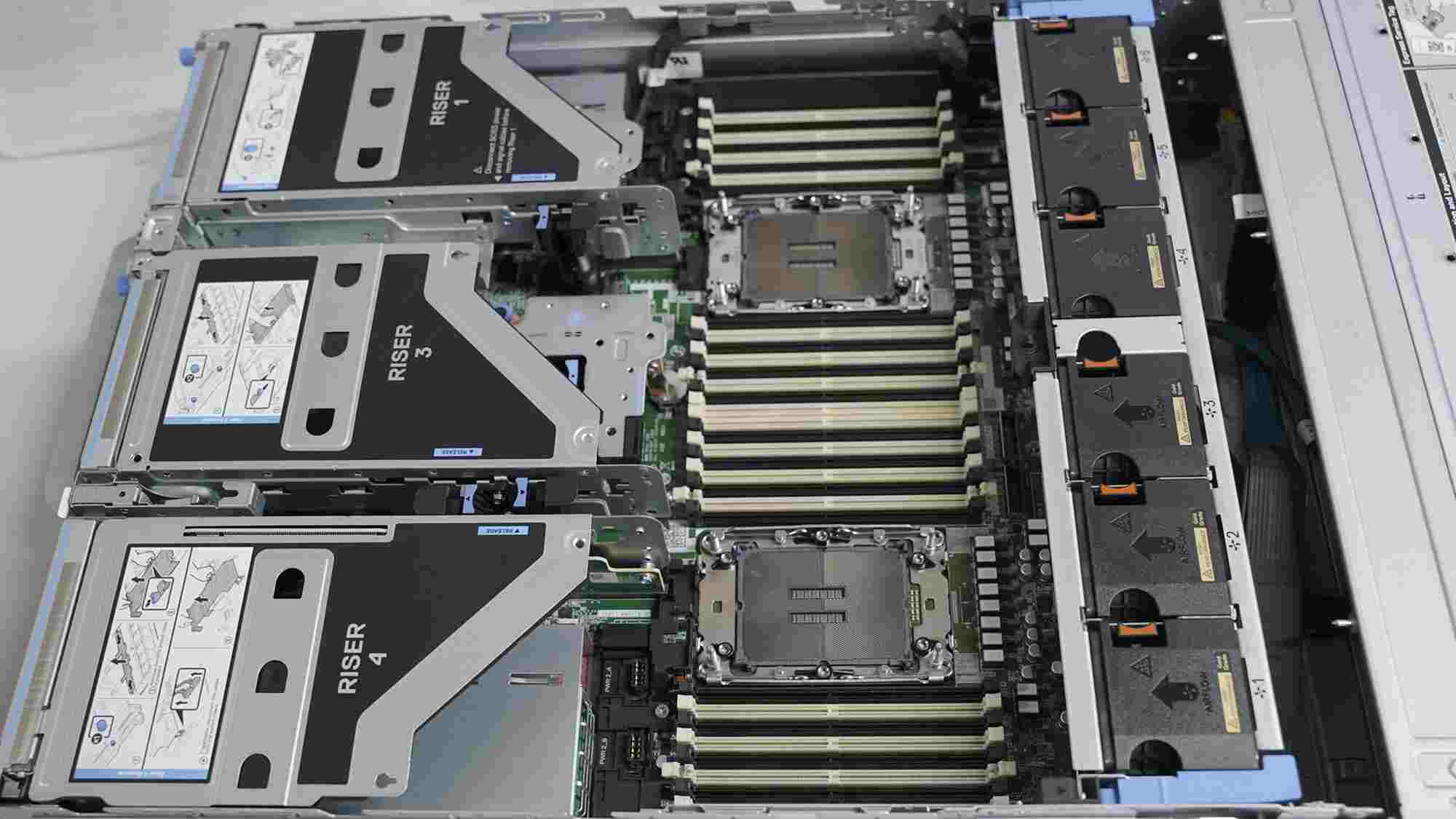
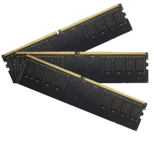
VoltDRAM Semiconductor Co., Ltd. is a professional manufacturer specializing in high-performance memory modules and electronic component solutions for servers, PCs, and data center applications. The company was registered between 2015–2018 and has rapidly developed into a reliable global supplier in the electronics and semiconductor memory industries.
Our manufacturing facility covers an area of approximately 320–480㎡, equipped with advanced production and testing lines. We generate an annual export revenue of around USD 8–18 million, with 6–9 years of export experience and 8–15 years of industry expertise in advanced electronics development and manufacturing.
Quality is at the core of VoltDRAM. We implement strict ISO-based quality management systems, combined with automated optical inspection (AOI), electrical performance testing, burn-in testing, and reliability stress testing to ensure stable product performance. Our quality control team consists of 35–80 experienced inspectors, ensuring every batch meets international standards.
With a strong international trade background, VoltDRAM mainly serves markets in North America, Europe, Southeast Asia, and the Middle East. We maintain long-term cooperation with over 600–1,500 supply chain partners, supporting a stable and efficient production ecosystem.
Our customers include OEM/ODM brands, system integrators, data center operators, and industrial computer manufacturers. We have strong R&D capabilities focused on high-speed system architecture optimization, signal integrity improvement, and power efficiency design. We also provide full customization options, including PCB design, memory capacity configuration, frequency tuning, and branding solutions.
Each year, we launch approximately 120–450 new product variants, supported by a dedicated R&D team of 60–300 engineers. Our innovation-driven approach allows us to continuously deliver competitive and high-performance memory and hardware solutions to global customers.


The step-by-step process required to build defect-free heavy copper printed circuit boards for industrial applications.
Beginning with high-Tg material sets (FR4/Polyimide), the base core is laminated with heavy-gauge copper foil under high pressure and heat to ensure trace adhesion.
Due to the thick copper walls, standard etching chemicals can cause severe undercutting. Special etchants and nozzle configurations are required to maintain straight sidewalls.
With thick copper features, standard prepreg cannot fill the deep gaps between traces. Vacuum-assisted resin filling prevents air pockets and electrical breakdown.
Finished boards undergo thermal shock tests, micro-sectioning, and high-voltage insulation tests to verify performance under demanding operational profiles.
Expert answers regarding heavy copper PCB design, pricing, standards, and global supply chain strategies.
Generally, any PCB containing copper weights above 3 oz/ft² (105 µm) on either internal or external layers is classified as heavy or thick copper. Boards exceeding 10 oz/ft² are classified as extreme heavy copper. They must comply with specific design rules regarding trace spacing and clearance to prevent defects during the etching process.
Yes. However, it requires careful stackup design. Prepreg materials with high resin content are necessary to fill the large gaps between thick copper traces. Combining standard copper layers (for signal routing) and thick copper layers (for power distribution) on the same board is standard practice, though it requires precise balancing of the stackup to prevent warp and twist during thermal processes.
Dual-sourcing combines local Canadian prototyping (for IP security and fast iterations) with scaled manufacturing from Chinese partners like VoltDRAM. This approach helps manage costs, mitigates supply chain risks, and ensures access to specialized materials that may not be readily available in domestic facilities.
As copper thickness increases, the required minimum trace width and spacing must also scale up. For example, a 1 oz copper layer can support 4 mil lines and spaces, while a 5 oz copper layer typically requires at least 15 to 20 mil lines and spaces to allow the etching chemistry to clear the paths completely without undercutting the traces.
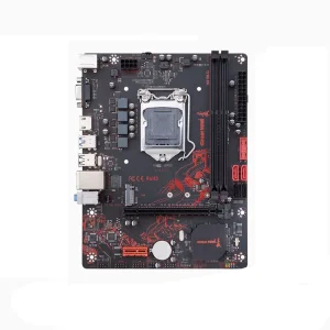
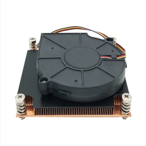
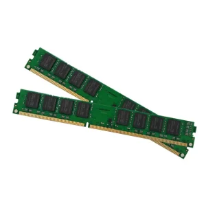
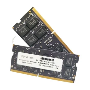
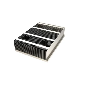
Explore our complete range of high-sensitivity circuits, desktop boards, cooling interfaces, and performance memory systems designed for rugged operating conditions.

Our engineers work directly with your design files (Gerber / ODB++) to optimize trace geometry, ensure thermal limits, and plan robust panelization for cost-effective manufacturing.
Send Inquiry Now