Engineered for high-frequency signal integrity, ultra-low thermal resistance, and seamless integration on SMT lines calibrated with precision laser stencils.
The electronics manufacturing services (EMS) landscape in the United States is undergoing a rapid, technology-driven renaissance. As local manufacturing reshores and capitalizes on the CHIPS Act, the demand for ultra-precise Surface Mount Technology (SMT) laser stencils has hit historic highs. In high-reliability sectors like military avionics, aerospace, medical devices (complying with stringent FDA standards), and high-performance automotive platforms, zero-defect solder paste deposition is the critical first step in the assembly process.
Modern SMT designs frequently pair fine-pitch micro-BGAs (0.3mm to 0.4mm pitch) alongside massive passive components like power inductors. This component disparity demands advanced step stencil technology (step-up and step-down stencils) to ensure that the correct volume of solder paste is distributed across every pad. Without precise stencil geometries and cutting-edge nano-coatings, manufacturing yields plummet due to bridging, tombstoning, and insufficient solder joints.
• Critical Area Ratio: Ensuring area ratios are kept > 0.66 for stable solder paste release on 0201 and 01005 components.
• Aperture Wall Smoothness: Under 1.5 micron Root-Mean-Square (RMS) roughness achieved using fiber lasers.
• Fiducial Alignments: High-contrast laser-etched half-etched or through-etched fiducials directly matching visual recognition algorithms of US-manufactured DEK, MPM, and Ekra stencil printers.
As an industry-leading manufacturing specialist, VoltDRAM Semiconductor Co., Ltd. serves the United States market by bridging advanced semiconductor-grade micro-testing methodologies with bulk production of fine-pitch, high-reliability laser-cut stencils. We configure customized stencil designs to match our clients' exact CAD footprints, ensuring high pass rates on automated optical inspections (AOI).
Understanding how materials, surface treatments, and cutting technologies dictate solder paste transfer efficiency on fine-pitch components.
We utilize SUS304 and specialized fine-grain (FG) stainless steel sheets. These metals exhibit uniform grain structures (1 to 5 microns) which prevent micro-cracks during laser exposure. Standard stainless steel stencils can cause jagged aperture walls, whereas FG sheets yield incredibly smooth walls that promote complete solder paste release.
Our state-of-the-art hydrophobic and oleophobic nano-coatings are chemically bonded to the stencil's underside and aperture walls. This process minimizes the solder paste friction coefficient, allowing for cleaner stencil release and reducing the required underscreen cleaning frequency from every 3 cycles down to 15+ cycles, boosting overall SMT throughput.
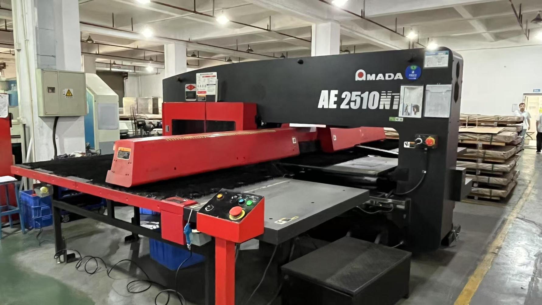
All stencils are fabricated using high-precision German LPKF fiber lasers. The laser spot size is kept under 20 microns, creating perfectly vertical aperture walls or slightly tapered designs (1-2 degrees) that optimize paste release. This precision guarantees accurate deposition for ultra-fine-pitch QFNs, BGAs, and 01005 passives.
| Stencil Parameter | Laser-Cut Stainless Steel | Laser-Cut Fine Grain (FG) | Electroformed Nickel Stencils |
|---|---|---|---|
| Typical Thickness | 0.08mm - 0.25mm (3mil - 10mil) | 0.08mm - 0.20mm (3mil - 8mil) | 0.025mm - 0.15mm (1mil - 6mil) |
| Aperture Tolerances | ±5.0 μm | ±3.0 μm | ±1.5 μm |
| Aperture Wall Roughness (Ra) | < 2.5 μm | < 1.5 μm | < 0.5 μm |
| Best for Component Size | Down to 0.5 mm pitch BGAs | Down to 0.4 mm pitch / 0201 Components | Down to 0.3 mm pitch / 01005 / Wafer bumping |
| Average Transfer Efficiency | 70% - 85% | 85% - 95% (with Nano-Coating) | 95% - 98% |
For procurement departments and hardware engineers in North America, sourcing custom SMT stencils and matching electronic components requires a fine balance of fast turnaround times, cost efficiency, and absolute reliability. While local US shops offer quick turnarounds, they struggle to match the competitive pricing models, advanced raw material reserves, and massive capacity scalability available at our advanced production facilities.
By integrating advanced digital workflows, our engineering team can review Gerber and CAD data files within hours, resolving potential manufacturing design flaws (using Gerber IPC-7525 checks) before cutting. Coupled with premium courier networks, we deliver custom-tailored stencils and matching semiconductor parts directly to your assembly lines in the US (from San Jose and Austin to Boston and Chicago) within 3 to 5 business days.
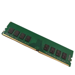
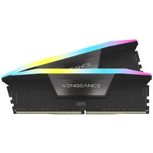
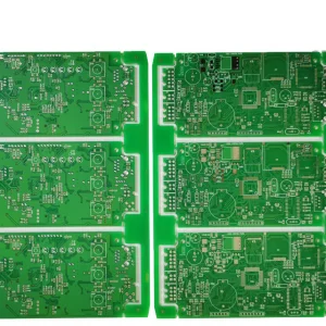
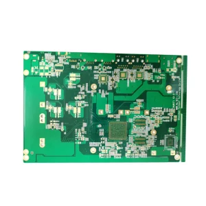
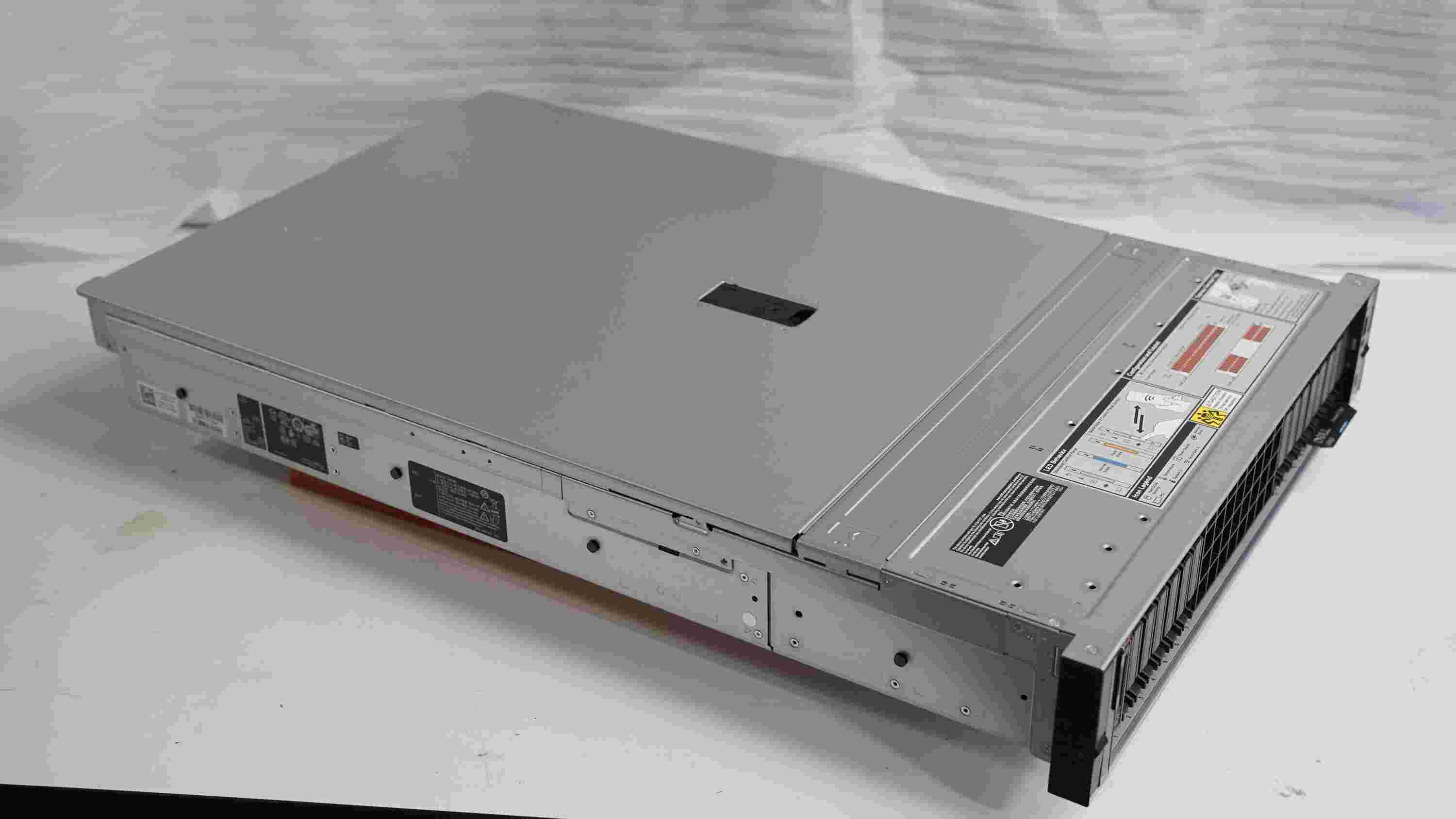
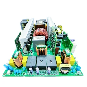
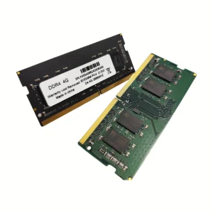
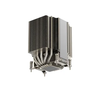
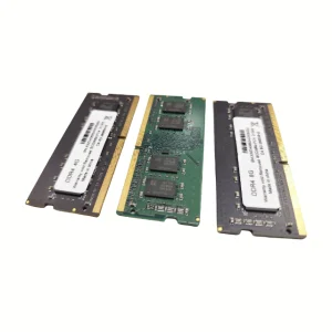
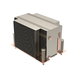
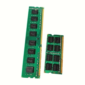
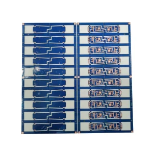
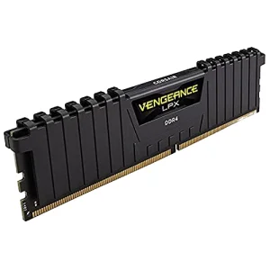
Furthermore, our integration with VoltDRAM Semiconductor Co., Ltd. allows us to offer dual-expertise. Not only do we manufacture stencils, but we also design, test, and supply high-performance DDR5/DDR4 DRAM modules, custom PCBs, and high-efficiency thermal cooling systems. This macro-level integration simplifies your supply chain, reducing transaction and shipping costs while ensuring consistent technical quality control.
Applying AOI, microscopic aperture measurement, and strict ISO-compliant QC oversight to all stencils.
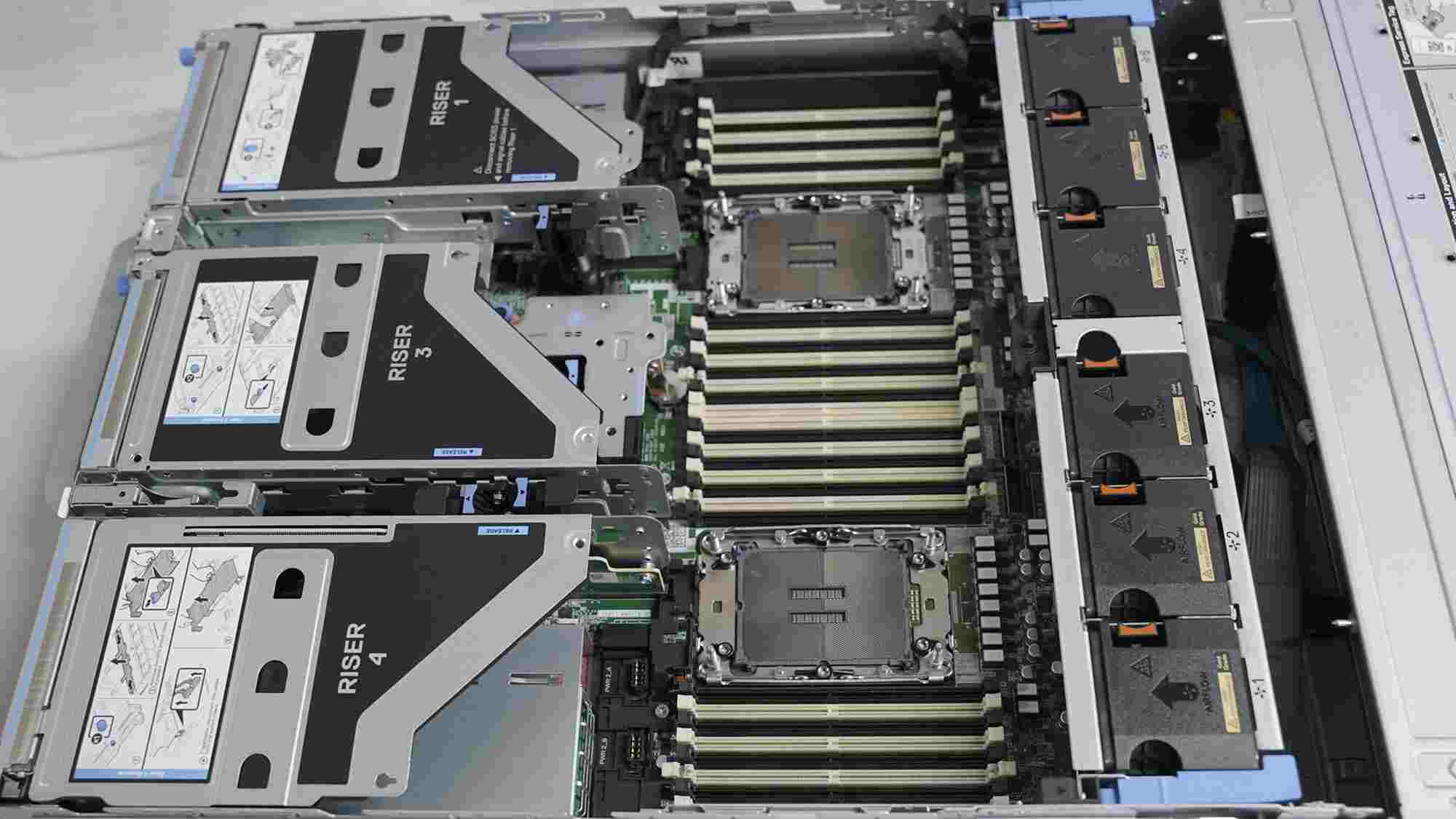
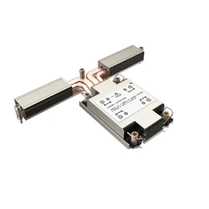
Coordinate stencils directly with PCBs, memory upgrades, and specialized server-grade heatsinks.
30% to 50% cost savings compared to domestic US quick-turns, even when accounting for fast air freight logistics.
We support custom space-saving frameless foils (Alpha Tetra, ZelFlex, LPKF ZelFlex ZP) and pre-framed profiles.
A trusted global supplier specializing in high-performance DRAM solutions, advanced semiconductor packaging, and micro-precision engineering.
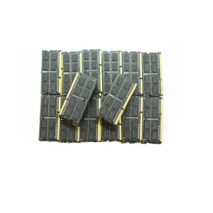
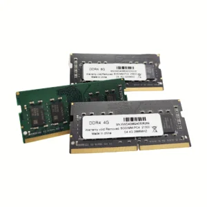
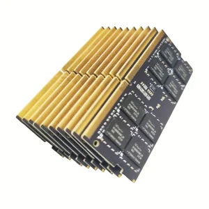
VoltDRAM Semiconductor Co., Ltd. is a professional DDR5 memory manufacturer specializing in high-performance DRAM solutions for servers, PCs, and data center applications. The company was registered between 2015–2018 and has rapidly developed into a reliable global supplier in the memory and high-precision electronic manufacturing industries.
Our manufacturing facility covers an area of approximately 320–480㎡, equipped with advanced production and testing lines. We generate an annual export revenue of around USD 8–18 million, with 6–9 years of export experience and 8–15 years of industry expertise in semiconductor memory development, high-frequency PCB board design, and micro-aperture laser profiling.
Quality is at the core of VoltDRAM. We implement strict ISO-based quality management systems, combined with automated optical inspection (AOI), electrical performance testing, burn-in testing, and reliability stress testing to ensure stable product performance. Our quality control team consists of 35–80 experienced inspectors, ensuring every batch meets international standards.
With a strong international trade background, VoltDRAM mainly serves markets in North America, Europe, Southeast Asia, and the Middle East. We maintain long-term cooperation with over 600–1,500 supply chain partners, supporting a stable and efficient production ecosystem.
Our customers include OEM/ODM brands, system integrators, data center operators, and industrial computer manufacturers. We have strong R&D capabilities focused on high-speed DDR5 architecture optimization, signal integrity improvement, and power efficiency design. We also provide full customization options, including PCB design, memory capacity configuration, frequency tuning, stencil matching, and branding solutions.
Each year, we launch approximately 120–450 new product variants, supported by a dedicated R&D team of 60–300 engineers. Our innovation-driven approach allows us to continuously deliver competitive and high-performance memory and component solutions to global customers.


Providing custom aperture geometry designs to fit the production lines of various industries.
Serving EV clusters in Michigan, Ohio, and California. Automotive electronic modules require high-reliability solder bonds under extreme temperature changes. Our stencils feature optimized thermal pad designs (windowpane patterns) to eliminate voids in massive heat sink areas, maintaining compliance with automotive assembly standards.
Supporting critical electronic medical assembly sites in Minnesota, Massachusetts, and Texas. For implants and monitor PCBs that require extremely tight packaging densities, we supply electroformed and nano-coated stencils that achieve excellent paste release down to 01005 component footprints.
Addressing high-speed server component needs in Oregon, Texas, and Virginia. High-frequency boards demand minimal signal attenuation. Combining VoltDRAM's custom RAM architectures with our precise step-stencils ensures clean joint formations on high-speed traces without signal integrity disruption.
Explore our full catalog of high-performance memory modules, thermal management systems, and precision PCB designs tailored for advanced electronics manufacturing.
Technical guidance from our senior engineering and assembly validation teams.
Under IPC-7525 guidelines, the Area Ratio (AR) is calculated as the area of the aperture opening divided by the surface area of the aperture walls. For a rectangular aperture of width (W) and length (L) on a stencil of thickness (T), the formula is AR = (W * L) / (2 * (W + L) * T). For reliable solder paste release, we target an AR > 0.66. For circular micro-BGAs, the calculation simplifies to AR = D / (4 * T) (where D is the diameter), targeting similar parameters.
Step-stencils are used when components require different volumes of solder paste on the same PCB. Step-down sections (e.g., reducing thickness from 5mil to 4mil) are used for fine-pitch components like 0.4mm BGAs to prevent bridging. Step-up sections (e.g., increasing from 5mil to 8mil) are utilized for large connectors or power modules that require extra solder volume for structural strength.
Hydrophobic nano-coatings repel flux solvents. When the stencil separates from the PCB, the coating prevents paste from sticking to the aperture walls and minimizes lateral squeeze-out on the stencil's underside. This decreases paste residue, resulting in fewer bridges, fewer stencil-cleaning cycles, and more consistent print volumes across high-volume production runs.
We accept standard ODB++ or Gerber data (RS-274X formats). To ensure high accuracy, we need the paste mask layers, solder mask layers, copper layers (for fiducial confirmation), and board outline profile. Our engineering team reviews all files to ensure compatibility with your specified stencil frame mount.
VoltDRAM utilizes systematic, multi-tiered testing protocols including automated optical inspection (AOI), high-temperature burn-in trials, and performance sweeps. Every batch of custom PCBs, memory modules, and micro-stencils is inspected by our quality assurance team to meet IPC Class 2 and Class 3 electronic standards.
Get in touch with our engineering and procurement team for custom stencil DFM analysis, technical pricing quotes, and quick-turn air shipments to the United States.
Send Inquiry Now