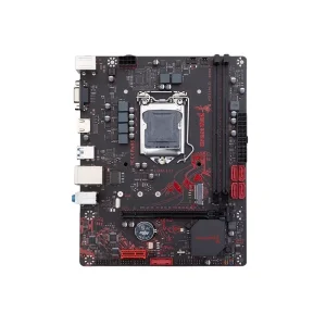
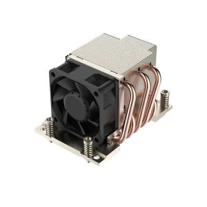
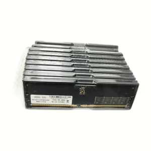
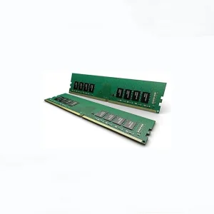
Discover the foundational server motherboards and cooling technologies engineered to integrate with high-precision SMT designs, utilizing state-of-the-art laser cut stencils for exact solder paste deposition.
In the heart of the Middle East, Doha, Qatar is undergoing a monumental shift. Under the roadmap of Qatar National Vision 2030, the nation is actively transitioning from a resource-dependent economy to a knowledge-based, high-tech industrial manufacturing hub. Key specialized economic zones, such as the Qatar Free Zones (QFZ) at Ras Bufontas and Umm Alhoul, alongside the Qatar Science & Technology Park (QSTP), are attracting global technology players. These investments have catalyzed localized SMT (Surface Mount Technology) assembly lines and hardware development projects.
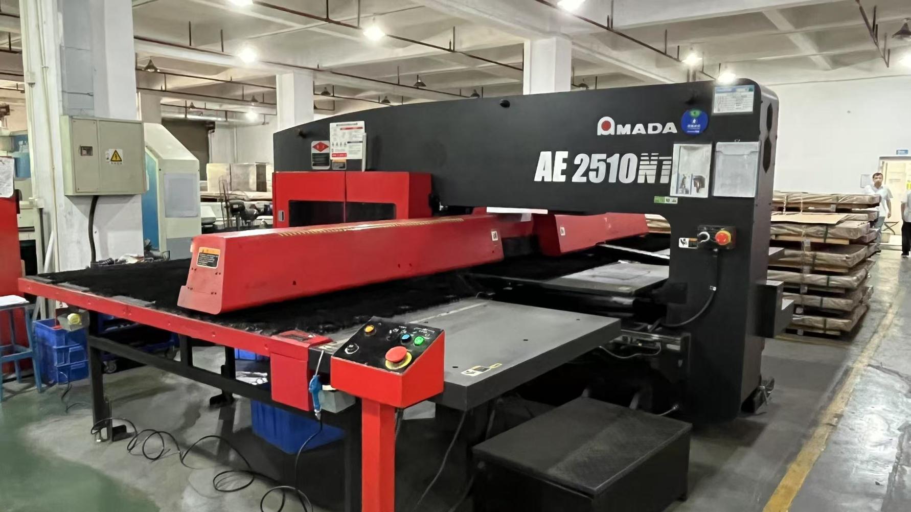
Precision SMT assembly begins with the stencil. Laser cut stencils are the primary tool used to govern the precise deposition of solder paste onto Printed Circuit Boards (PCBs). In Doha's challenging desert climate—where temperature and relative humidity must be stringently regulated inside cleanrooms—minor anomalies in solder paste viscosity can cause catastrophic bridge defects or voids. By utilizing laser stencils constructed from high-tensile stainless steel with specialized nano-coatings, local engineers achieve optimal paste release, minimizing production downtime for industrial infrastructure, aerospace systems, and localized IoT hardware.
Doha's local electronics manufacturing demands precision to combat climatic challenges. To maintain high-yield rates for high-speed processors and dense memory footprints, manufacturers implement standard calculations:
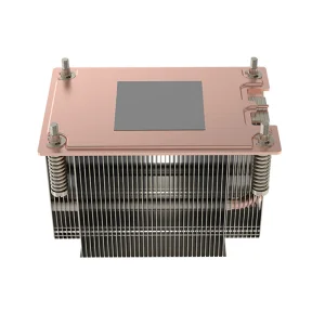
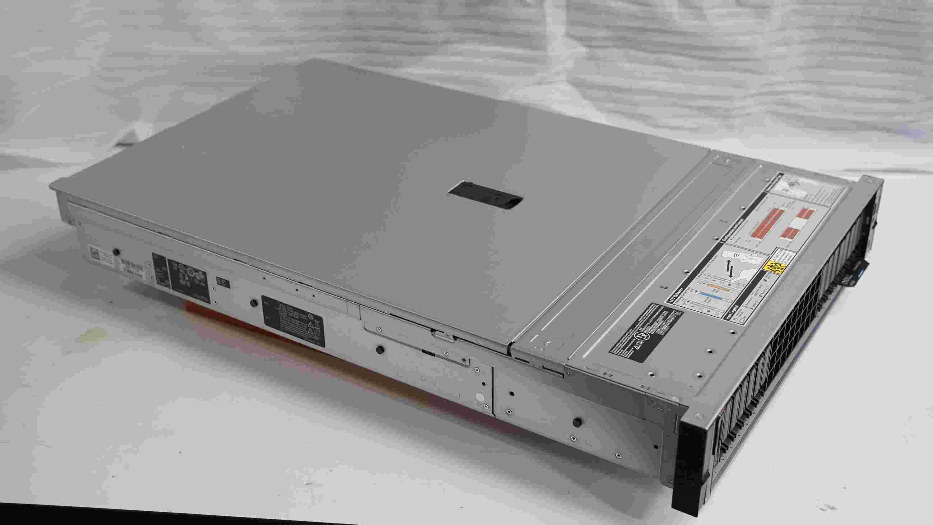
High-density server components require reliable passive cooling structures and advanced multi-channel logic boards. These boards are assembled using premium laser stencils to ensure strict coplanarity of BGA pads.
Precision stenciling is not just a tool; it is the core determinant of reliability in hardware assembly across global industries.
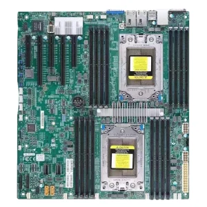
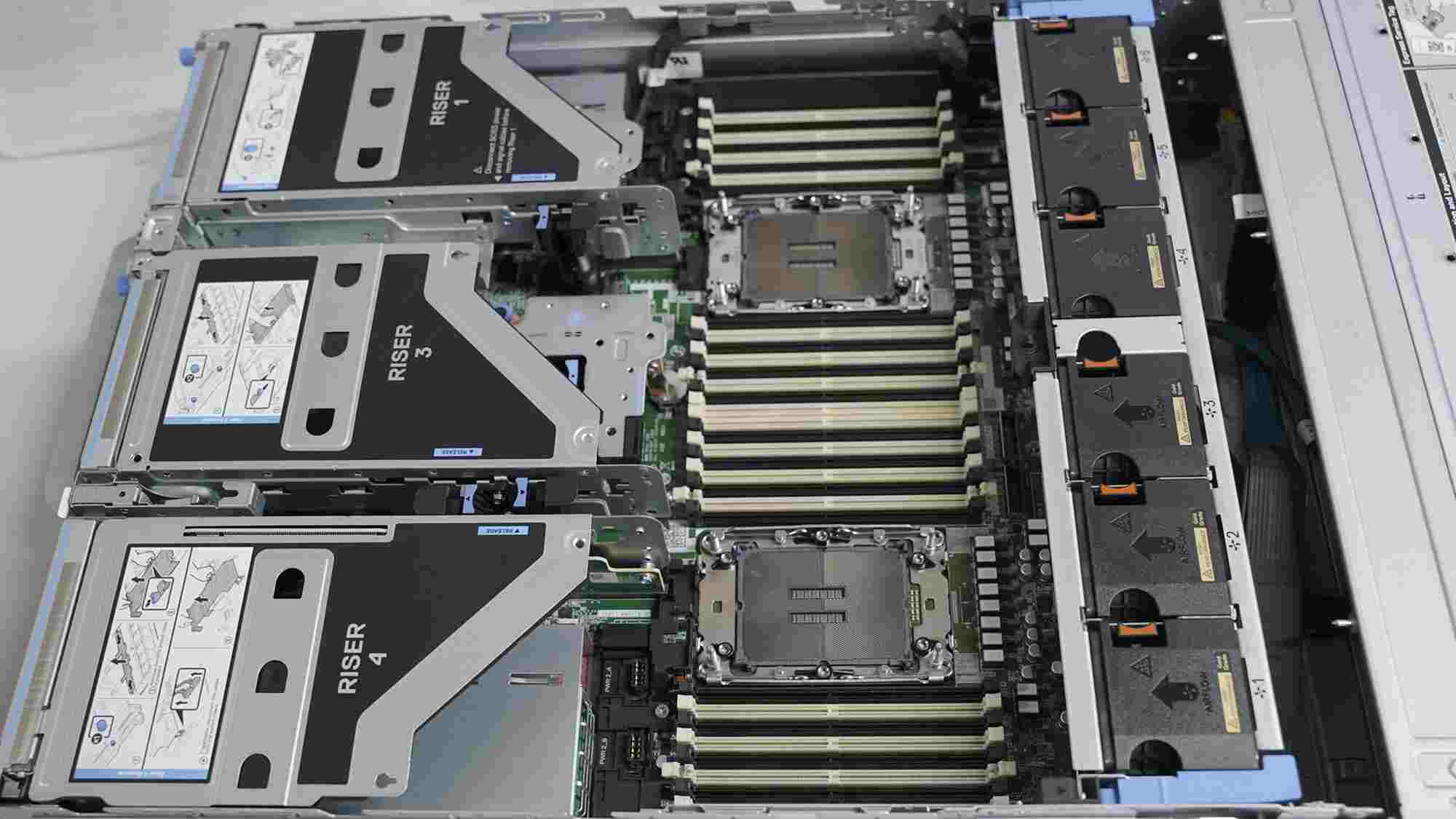
Modern server units, including motherboard architectures running Xeon or AMD EPYC platforms, require high-frequency multi-layer PCBs. Any minor soldering defect under a 1000+ pin BGA package leads to high scrap rates. Laser stencils with electro-polished walls and nano-coatings guarantee defect-free solder deposition, keeping data corridors in Qatar's new cloud zones fully operational.
Doha is a major hub for liquefied natural gas (LNG). Industrial process control units placed near extraction points operate under severe heat, shock, and vibration. These boards require heavy copper traces and stepped stencils (combining varying foil thicknesses on a single frame) to deposit different volumes of solder for heavy power components and ultra-fine pitch control ICs.
Smart city grids in Lusail rely on decentralized AI compute units. These units contain high-frequency DDR5 RAM and deep neural accelerators. Fabricating these devices necessitates step-down stencils with microscopic aperture tolerances, ensuring zero solder balling and pristine thermal pad interfaces.
To support next-generation semiconductor packages like 0.3mm pitch CSPs (Chip Scale Packages) and high-density 01005 passives, stencil manufacturing has evolved through three major technological milestones:
As assembly sizes contract and system-in-package (SiP) designs gain dominance, the global stencil manufacturing ecosystem is shifting toward smart, automated production. The integration of SPI (Solder Paste Inspection) feedback loops directly communicates with the stencil cleaning cycle, allowing automated machines to clean residues before defects arise.
Additionally, the adoption of hydrophobic and flux-phobic nano-coatings (such as Self-Assembled Monolayers - SAM) has transitioned from a premium option to an industrial requirement. These nano-coatings, measuring only a few nanometers in thickness, prevent solder paste from adhering to the underside and walls of the stencil, resulting in up to a 70% reduction in clean cycles and a massive reduction in bridge defects during high-speed production runs.
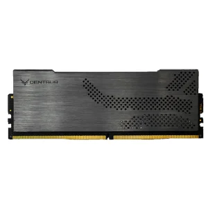
VoltDRAM Semiconductor Co., Ltd. is a professional DDR5 memory manufacturer specializing in high-performance DRAM solutions for servers, PCs, and data center applications. Operating in the hardware manufacturing ecosystem, our production depends heavily on the highest quality SMT practices and precision laser stencils.
Quality is at the core of VoltDRAM. We implement strict ISO-based quality management systems, combined with automated optical inspection (AOI), electrical performance testing, burn-in testing, and reliability stress testing to ensure stable product performance. Our quality control team consists of 35–80 experienced inspectors, ensuring every batch meets international standards.
With a strong international trade background, VoltDRAM mainly serves markets in North America, Europe, Southeast Asia, and the Middle East. We maintain long-term cooperation with over 600–1,500 supply chain partners, supporting a stable and efficient production ecosystem. Our customers include OEM/ODM brands, system integrators, data center operators, and industrial computer manufacturers.
We have strong R&D capabilities focused on high-speed DDR5 architecture optimization, signal integrity improvement, and power efficiency design. We also provide full customization options, including PCB design, memory capacity configuration, frequency tuning, and branding solutions. Each year, we launch approximately 120–450 new product variants, supported by our engineering teams. VoltDRAM is committed to becoming a trusted global partner in the DDR5 memory industry, delivering stable, fast, and efficient memory products for the next generation of computing systems.


Find answers to the most critical technical questions regarding laser stencils and industrial electronics assembly in Qatar.
Typically, custom laser stencils are fabricated and verified using optical inspection within 24 to 48 hours of Gerber file approval. Utilizing express logistics partners, stencils reach production facilities in Doha (including Qatar Free Zones) within 3 to 5 business days, complete with mounting frames and protective packaging.
Doha's high outdoor temperatures and seasonal humidity fluctuations require strict temperature (21-25°C) and humidity (35-55% RH) control inside SMT cleanrooms. High ambient temperature degrades solder paste viscosity, causing slumping and bridging. Under these conditions, stencils with hydrophobic nano-coatings are highly recommended, as they prevent paste accumulation on the aperture walls and the stencil underside.
Step stencils are required when a single PCB houses both large-pad components (like power connectors, chokes, or high-power transistors) and fine-pitch modules (such as BGA packages, 0201 passives, or high-density memory chips). A Step-Up stencil locally increases thickness to provide more solder volume, whereas a Step-Down stencil reduces thickness to prevent shorts on microscopic chip contacts.
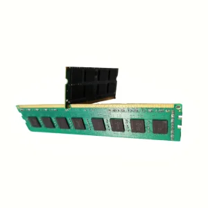
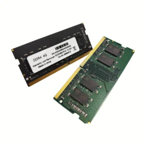
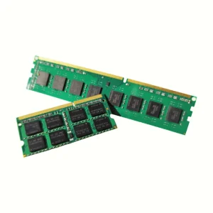
VoltDRAM DDR5 and ECC DDR4 memory modules are designed using industry-standard PCB layouts with fiducial marks optimized for automated optical alignment. Our strict manufacturing guidelines define recommended solder paste volume and stencil aperture design templates, ensuring that local system integrators in Doha can achieve 100% solder joint reliability during reflow.
Yes. Stencils can be supplied either as frameless foils (ideal for space-saving storage and use with reusable pneumatic quick-tension systems like LPKF ZelFlex) or pre-mounted on aluminum frames (standard sizes: 23"x23", 29"x29") to fit directly into major automated stencil printers like DEK, MPM, or GKG.
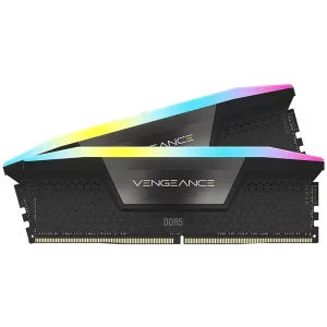
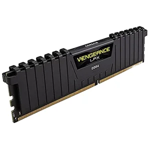
These performance-grade products require precise stencil patterns to ensure perfect connection interfaces on modern high-speed motherboards and server rack systems.